
Solar energy has emerged as a leading renewable energy source, with solar panels playing a crucial role in harnessing the power of the sun. As the demand for clean energy grows, it’s essential to understand the core materials and manufacturing processes that go into creating these innovative devices. In this comprehensive article, we’ll delve into the key components of solar panels and explore the cutting-edge technologies used in their production.
The Building Blocks of Solar Panels
Solar panels are composed of several critical components that work together to convert sunlight into usable electricity. Let’s take a closer look at these essential elements:
1. Photovoltaic Cells: The Heart of Solar Panels
At the core of every solar panel lie photovoltaic (PV) cells, which are responsible for the photovoltaic effect – the process of converting light into electrical energy. These cells are typically made from semiconductor materials, such as silicon, that absorb sunlight and generate an electric current.
How PV Cells Work:
- Sunlight, composed of photons, strikes the PV cell.
- The photons are absorbed by the semiconductor material, typically silicon.
- The absorbed photons knock electrons loose from their atoms, creating an electric current.
- The electric current is captured by metal contacts on the top and bottom of the cell, which channel the electricity out of the cell for use.
2. Crystalline Silicon: The Dominant Material
Crystalline silicon is the most widely used material in solar panel manufacturing, accounting for over 90% of the global market. There are two main types of crystalline silicon cells:
- Monocrystalline Silicon: Known for its high efficiency and sleek appearance, monocrystalline silicon is made from a single crystal of pure silicon. These cells are more expensive to produce but offer superior performance compared to other types. The manufacturing process involves growing a single crystal of silicon, which is then cut into wafers for cell production.
- Polycrystalline Silicon: Manufactured using multiple silicon crystals, polycrystalline cells are less efficient than their monocrystalline counterparts but offer a more cost-effective solution. The polycrystalline silicon manufacturing process involves melting and casting silicon into square molds, resulting in a distinctive speckled appearance. While less efficient, polycrystalline panels are more affordable and have a lower carbon footprint during production.
Comparison of Monocrystalline and Polycrystalline Silicon:
| Feature | Monocrystalline | Polycrystalline |
|---|---|---|
| Efficiency | Higher (15-22%) | Lower (13-16%) |
| Appearance | Uniform, dark color | Speckled, blue hue |
| Cost | More expensive | More affordable |
| Lifespan | 25-30 years | 20-25 years |
| Temperature Coefficient | Lower (better performance in high temperatures) | Higher (reduced performance in high temperatures) |
3. Thin-Film Technologies: An Emerging Alternative
While crystalline silicon dominates the solar panel market, thin-film technologies are gaining traction as a promising alternative. These ultra-thin layers of photovoltaic materials, such as cadmium telluride (CdTe), copper indium gallium selenide (CIGS), and amorphous silicon (a-Si), offer several advantages, including flexibility, lightweight design, and reduced material costs. However, thin-film panels generally have lower efficiency rates compared to crystalline silicon.
Advantages of Thin-Film Solar Panels:
- Flexibility: Thin-film panels can be bent and shaped to fit various surfaces, making them ideal for applications such as solar-powered vehicles and portable devices.
- Lightweight: The thin, lightweight nature of these panels makes them easier to transport and install, reducing overall system costs.
- Low Light Performance: Thin-film panels perform better in low light conditions and are less affected by shading compared to crystalline silicon panels.
- Aesthetics: The uniform, black appearance of thin-film panels can be more visually appealing for certain applications, such as building-integrated photovoltaics (BIPV).
Despite these advantages, thin-film panels have lower efficiency rates (5-13%) compared to crystalline silicon, requiring more space to generate the same amount of electricity. Additionally, some thin-film materials, such as cadmium, raise concerns about toxicity and environmental impact during production and disposal.
The Solar Panel Manufacturing Process
Creating a solar panel involves a series of intricate steps, from raw material processing to final assembly. Here’s a detailed overview of the manufacturing process:
- Silicon Purification: The journey begins with the purification of raw silicon, which is typically obtained from quartz sand. The silicon is heated in an electric arc furnace to temperatures above 1,800°C (3,272°F), causing a chemical reaction that removes impurities and produces metallurgical-grade silicon with a purity of around 99%. This metallurgical-grade silicon is then further purified using the Siemens process or the fluidized bed reactor (FBR) process to achieve the ultra-high purity (99.9999% or higher) required for solar cell production.
- Ingot and Wafer Production: The purified silicon is melted and formed into a large crystal, called an ingot, using either the Czochralski method (for monocrystalline silicon) or the casting method (for polycrystalline silicon). The Czochralski method involves slowly pulling a seed crystal from a vat of molten silicon, allowing a single crystal to grow. The casting method involves pouring molten silicon into a square mold and allowing it to cool and solidify. The resulting ingots are then sliced into thin wafers, typically 150-200 micrometers thick, using precision wire saws or diamond wire saws.
- Cell Fabrication: The silicon wafers undergo a series of treatments to enhance their ability to absorb sunlight and generate electricity. These steps include:
- Surface Texturing: The wafer surface is etched with tiny pyramids or other patterns to reduce reflectivity and increase light absorption.
- Doping: The wafer is exposed to impurities (usually boron and phosphorus) to create a positive-negative (p-n) junction, which is essential for generating an electric current.
- Anti-Reflective Coating: A thin layer of silicon nitride or titanium dioxide is applied to the wafer surface to further reduce reflectivity and improve light absorption.
- Metallization: Metal contacts, typically silver or aluminum, are screen-printed onto the front and back of the cell to collect and transport the generated electricity.
- Cell Interconnection: Individual solar cells are interconnected using thin, flat wires or metal ribbons to form a complete solar panel circuit. The cells are typically arranged in a grid pattern, with the front of one cell connected to the back of the adjacent cell. This series connection allows the electrical energy to flow through the entire panel.
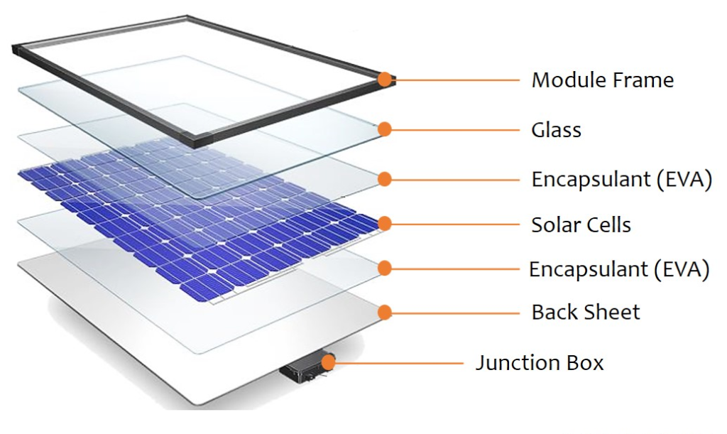
- Encapsulation and Lamination: The interconnected cells are encapsulated in a protective layer to shield them from environmental factors such as moisture, dust, and extreme temperatures. The most common encapsulant material is ethylene-vinyl acetate (EVA), which is laminated to the front and back of the cell matrix using heat and pressure. A tempered glass sheet is placed on the front of the panel to provide additional protection and structural support, while a polymer backsheet, typically made of Tedlar or polyvinyl fluoride (PVF), is added to the back for insulation and weatherproofing.
- Framing and Junction Box Installation: The laminated panel is then framed with aluminum to increase its structural integrity and facilitate mounting. A junction box, which houses the panel’s electrical connections and bypass diodes, is attached to the back of the panel. The bypass diodes help prevent power loss in case of partial shading or cell damage.
- Quality Control and Testing: Each solar panel undergoes rigorous quality control checks and performance testing to ensure it meets industry standards and manufacturer specifications. These tests include:
- Visual Inspection: Panels are inspected for any visible defects, such as cracks, scratches, or discoloration.
- Electrical Performance Testing: Panels are tested under standard test conditions (STC) to measure their power output, efficiency, and other electrical parameters.
- Environmental Testing: Panels are subjected to various environmental stresses, such as extreme temperatures, humidity, and mechanical loads, to assess their durability and reliability.
- Electroluminescence (EL) Imaging: This non-destructive testing method uses an infrared camera to detect micro-cracks, inactive areas, and other defects in the solar cells that may not be visible to the naked eye.
Panels that pass these quality control checks are then packaged and shipped to customers for installation.
Advancements in Solar Panel Technology
The solar industry is continuously evolving, with researchers and manufacturers developing new technologies to improve the efficiency, durability, and cost-effectiveness of solar panels. Some notable advancements include:
- PERC (Passivated Emitter and Rear Cell) Technology: PERC is a cell design that adds a reflective layer to the back of the cell, allowing more light to be captured and converted into electricity. This technology has the potential to boost solar panel efficiency by up to 5% compared to conventional cells. PERC cells also perform better in low light conditions and at higher temperatures, making them a popular choice for residential and commercial installations.
- Bifacial Solar Panels: These innovative panels can capture sunlight from both sides, increasing energy production by up to 30% compared to traditional monofacial panels. Bifacial panels are particularly useful in installations where sunlight can be reflected off the ground or surrounding surfaces, such as on flat commercial rooftops or in solar farms with light-colored gravel or snow. The dual-sided design also allows for vertical installation, which can be advantageous in space-constrained areas or for architectural purposes.
- Solar Tracking Systems: Solar tracking systems allow panels to follow the sun’s path throughout the day, optimizing their orientation for maximum energy capture. There are two main types of tracking systems:
- Single-Axis Trackers: These systems rotate the panels along one axis (usually east to west) to follow the sun’s daily path across the sky.
- Dual-Axis Trackers: These more advanced systems rotate the panels along two axes (east to west and north to south) to precisely track the sun’s position, maximizing energy production. Solar tracking systems can increase energy production by up to 40% compared to fixed-tilt installations, making them an attractive option for large-scale solar farms and commercial projects.
- Half-Cell Technology: Half-cell panels are created by cutting standard solar cells in half, resulting in two smaller cells that are connected in parallel. This design offers several advantages:
- Reduced Electrical Losses: By halving the current in each cell, half-cell panels experience lower electrical resistance and reduced power losses, leading to higher overall panel efficiency.
- Improved Shading Performance: If a portion of a half-cell panel is shaded, only the affected half-cells will experience reduced output, while the unshaded half-cells continue to perform optimally. This results in better overall panel performance under partial shading conditions.
- Enhanced Durability: Half-cell panels exhibit lower heat stress and reduced mechanical stress, as the smaller cells are more resistant to cracking and breakage. This increased durability can lead to longer panel lifetimes and reduced maintenance costs. Half-cell technology is becoming increasingly popular in residential and commercial solar installations, as it offers a balance of improved performance, reliability, and cost-effectiveness.
These advancements, along with others such as multi-junction cells, perovskite materials, and concentrator photovoltaics (CPV), are driving the solar industry forward and making solar energy an increasingly competitive and attractive option for power generation.
Environmental Impact and Recycling
As the world shifts towards sustainable energy solutions, it’s crucial to consider the environmental impact of solar panels throughout their lifecycle. While solar energy is clean and renewable, the production of solar panels does involve the use of raw materials and energy-intensive processes.
Environmental Concerns:
- Raw Material Extraction: The production of solar panels requires the mining and processing of raw materials such as silicon, silver, and aluminum. These activities can have negative environmental impacts, such as habitat destruction, water pollution, and greenhouse gas emissions.
- Energy Consumption: The manufacturing process for solar panels is energy-intensive, particularly the purification of silicon and the fabrication of cells and modules. This energy consumption contributes to the overall carbon footprint of solar panels.
- Hazardous Materials: Some solar panel technologies, such as thin-film panels, contain hazardous materials like cadmium and lead. If not properly handled and disposed of, these materials can pose risks to human health and the environment.
Despite these concerns, the solar industry is making significant strides in reducing its environmental footprint. Manufacturers are increasingly adopting circular economy principles, focusing on the recycling and reuse of solar panel components. Many companies now offer recycling programs for end-of-life panels, recovering valuable materials such as silicon, glass, and metals for use in new products.
Solar Panel Recycling Process:
- Collection and Transportation: End-of-life solar panels are collected from installation sites and transported to recycling facilities.
- Disassembly: Panels are dismantled, separating the glass, metal frames, junction boxes, and solar cells.
- Material Separation: The various components are further separated and sorted by material type (e.g., glass, silicon, metals).
- Material Processing: The separated materials are then processed for reuse:
- Glass: Crushed and cleaned for use in new glass products or as an aggregate in construction materials.
- Metals: Smelted and refined for use in new products.
- Silicon: Purified and reclaimed for use in new solar cells or other electronics.
- Disposal: Any remaining non-recyclable materials are safely disposed of in accordance with local regulations.
By recycling solar panels, the industry can reduce its reliance on raw materials, minimize waste, and decrease the overall environmental impact of solar energy production.
Additionally, the energy payback time (EPBT) of solar panels – the time it takes for a panel to generate the amount of energy used in its production – has significantly decreased in recent years. Modern solar panels typically have an EPBT of 1-4 years, depending on the technology and location, meaning they generate clean energy for the majority of their 25-30 year lifespan. As panel efficiencies continue to improve and manufacturing processes become more sustainable, the EPBT is expected to decrease further, making solar an even more environmentally friendly energy option.
Conclusion
Solar panels are a testament to human ingenuity and our ability to harness the power of the sun for clean, renewable energy. By understanding the core materials and manufacturing processes behind these remarkable devices, we can appreciate the technological advancements that have made solar energy a viable and increasingly accessible option for homes and businesses worldwide.
As the solar industry continues to evolve, we can expect to see even more innovative and sustainable solutions in the future. From maximizing solar panel efficiency to developing new materials and recycling technologies, the possibilities are endless. By embracing solar energy and supporting the growth of the solar industry, we can work towards a cleaner, greener future for generations to come.
Key Takeaways:
- Solar panels are composed of photovoltaic cells, typically made from crystalline silicon or thin-film materials, that convert sunlight into electricity.
- Monocrystalline and polycrystalline silicon are the most common materials used in solar panels, each with its own advantages and disadvantages.
- The solar panel manufacturing process involves a series of steps, from raw material processing to final assembly and quality control testing.
- Advancements in solar panel technology, such as PERC, bifacial panels, solar tracking systems, and half-cell technology, are improving the efficiency, durability, and cost-effectiveness of solar energy.
- The solar industry is addressing environmental concerns by adopting circular economy principles, focusing on recycling and reuse of solar panel components, and reducing the energy payback time of panels.
By investing in solar energy and supporting the continued development of solar panel technology, we can create a more sustainable future powered by clean, renewable energy from the sun.